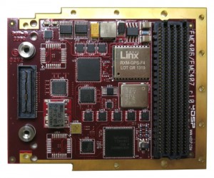
High-Speed Clocking Module – Low-Pin-Count
The FMC407 is a low-noise clock generation and distribution module with eight clock outputs and eight trigger outputs that are fully synchronized. This module can either distribute an externally supplied or a locally generated clock. In the standard configuration, the FMC407 can generate any clock frequency between 34.375 MHZ and 4.4GHz and lock it to an internal or external reference.
A synchronous trigger signal received from either the FMC connector or the external trigger input is distributed to the eight trigger outputs. Alternatively, it is also possible to distribute the external 1PPS or locally generated 1PPS signal for data time stamping. The FMC407 is recommended for applications that require synchronous A/D or D/A sampling across multiple cards or systems. With a low-pin count connector and front panel I/O, this module can be used in a conduction-cooled environment.
The design is based on Analog Devices’ ADF4351 PLL synthesizer in combination with the ADCLK954 LVPECL fan-out buffer. The  fan-out buffer outputs eight phase-aligned, low-noise clocks generated from either the external or internal clocks. A GPS module, the LINX RXM-GPS-F4-T, provides a 1PPS signal for clock and trigger synchronization. The FMC407 daughter card is mechanically and electrically compliant with the FMC standard (ANSI/VITA 57.1).
Features:
- External clock input and onboard VCO
- External reference input and onboard reference (30.72MHz)
- External 1PPS, Sync, and Trigger inputs
- Eight synchronized clock outputs (34.375MHz-4.4GHz)
- Eight synchronized trigger or 1PPS outputs
- Onboard GPS receiver for accurate data time stamping
- Fully controllable from FMC connector
- VITA 57.1-2010 compliant
- LPC (Low-Pin Count) 160-Pin Connector
- Mil-I-46058c Conformal Coating Compliant – Optional
- A breakout cable on the front panel makes all clock and trigger signals available on individual SMA sockets.

