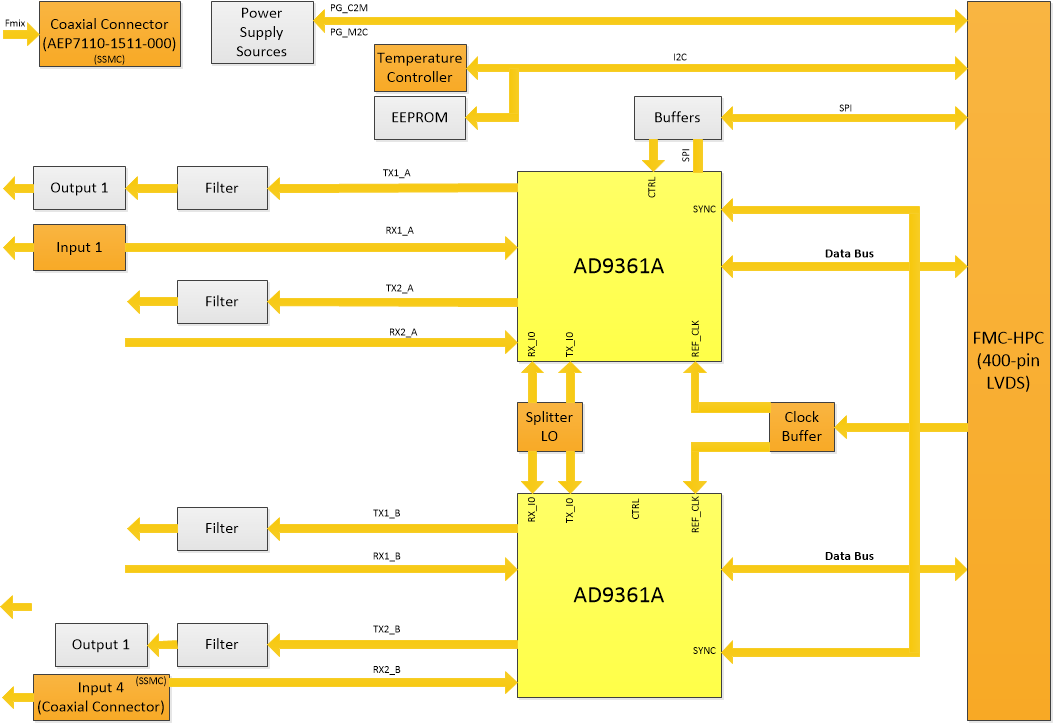
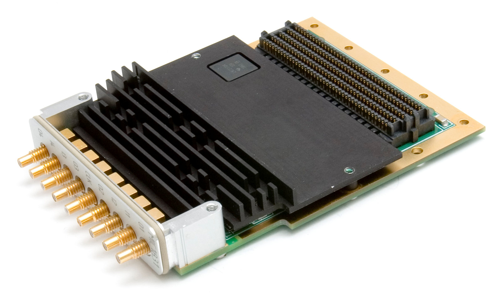
The FMC1831 is an FMC module designed to be compatible with AMC, VPX, PCI, PCIe, CompactPCI and PC/104 carriers. The module has two dual channel AD9361 transceivers with a maximum sampling frequency of 122.8 MHz over a bandwidth of 200 KHz to 56 MHz. A reference clock can be either externally supplied or be generated from an internal PLL. All input and output signals are connected via SSMC connectors for secure connectivity and signal integrity.
Functional Structure of the Module
- A set of secondary power supplies for all module blocks
Connector FMC HPC (ASP-134487-01):
- Input of 12P0V power supply lines, 3P3V, 3P3VAUX and Vadj
- I2C interface with carrier board
- Input and output of reference clock signals and signal synchronization
- Input / output of digital data buses between the carrier-board on chips of the transceivers, including tracking cycles and the signal of frames.
Transceivers:
- 1 or 2 AD9361 chip, depending on the version;
- Maximum sampling frequency fs, 122.8MGHz in case of the 1T1R configuration;
- 12 bits of input/output data;
- The range of readjustment of the mixing unit’s reference signal (using the internal synthesizer) – 70-6000 MHz;
- The range of readjustment of the mixing unit’s reference signal (using an external signal) – 70-4000 MHz;
- Input / output data standard – LVDS / CMOS;
- Data bus configuration – 1R1T, 1R2T, 2R1T, 2R2T;
- Modes of data bus operation – Single Port Half Duplex, Single Port Full Duplex, Dual Port Half Duplex, Dual Port Full duplex;
- Data format – offset binary code
- Data repetition frequency – fs – 4 * fs
Analog output filters:
- Selection of the filter type and its characteristics, in accordance with the version;
- Nomenclature of the filters to be installed is represented by LPF, High-pass and bandpass filters Mini-Circuits series LFCN, HFCN and BFCN, respectively
Connector for analog signals:
- SSMC AEP 7110-1511-000
Clocking circuit:
- The clock buffer ADCLK846 chip for distribution of reference frequency of the digital portion of transceivers
- Buffer on the NB7VQ14M chip for distributing the mixing unit’s signal
Chip of the non-volatile EEPROM memory:
- AT24C512C microchip with a volume of 512Kbit for storing service and identification information on the mezzanine.
Block Diagram