
 2-Channel ADC Module – High-Pin-Count
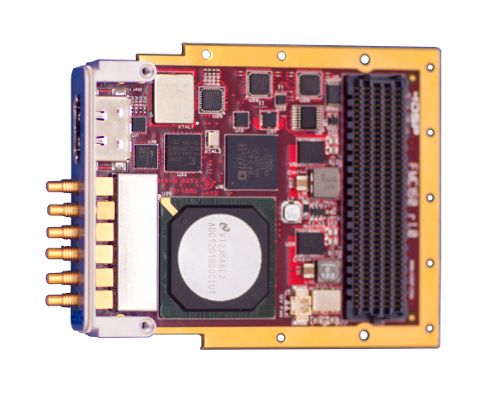
The FMC161 provides one 12-bit A/D channel at 3.6Gsps or two A/D channels at 1.8Gsps clocked by either an internal clock source (optionally locked to an external reference) or an externally supplied sample clock. In addition, a trigger input for customized sampling control is available to users. The FMC161 daughter card is mechanically and electrically compliant to the FMC standard (ANSI/VITA 57.1).
The FMC161 has a high-pin count connector, front panel I/O, and can be used in a conduction cooled environment. The design is based on Texas Instruments’ ADC12D1800 Analog-to-Digital converter. The analog signals are AC coupled connecting to MMCX or SSMC coax connectors on the front panel.
The FMC161 allows flexible control on clock source through serial communication busses. Furthermore the card is equipped with power supply and temperature monitoring and offers several power-down modes to switch off unused functions in order to reduce system level power consumption. It is well suited for low power applications such as airborne where the highest level of performance is required while ensuring that mission range does not get affected.
Features:
- One ADC12D1800: Single channel 12-bit 3.6Gsps or dual channel at 1.8Gsps
- VITA 57.1-2010 compliant
- Conduction Cooled – Standard Option
- Single ended AC-coupled analog signals
- 5 MMCX/SSMC connectors available from the front panel
- 4 LVTTL signals available from an HDMI connector on the front panel
- 4 Xilinx MGT available from an HDMI connector on the front panel
- Clock Source, Sampling Frequency through SPI communication busses
- Flexible clock tree enables:
- on board VCO: 2200MHz – 4400MHz
- external reference clock
- external sampling clock
- Power-down modes to switch off unused functions for system power savings
- Mil-I-46058c Conformal Coating Compliant (optional)
- HPC – High Pin Count Connector
- LVDS IO signaling