Single Board Computer with Intel Atom® E39XX processor and Intel Cyclone® V FPGA for swap applications
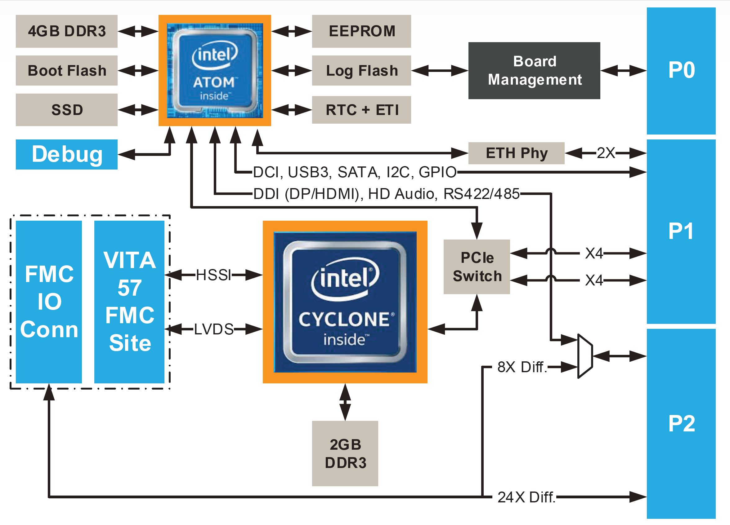
The VF370 is a 3U OpenVPX Single Board Computer (SBC) module that utilises the Intel Atom® E39xx series of embedded processors, Intel Cyclone® V FPGA technology and a FMC mezzanine site, to provide a module with scalable processing power and flexible IO options for reduced Size, Weight and Power (SWaP) applications. It is available in standard air-cooled and rugged conduction-cooled versions.
The single, dual and quad core Intel Atom® E39xx processors offer enhanced processing power in a compact, lowpower package running at speeds of up to 2.0 GHz. It delivers enhanced reliability in extreme environments typically found in industrial, automotive and aerospace applications.
The integrated graphics processor (running at up to 650 MHz) achieves greatly increased video encode and playback performance, with Ultra HD 4K display resolution on multiple independent displays for surveillance and other video centric applications.
Intel® Time Coordinated Computing Technology (Intel® TCC Technology) can synchronise networks of devices to within 1 μs, greatly improving the realtime deterministic behaviour of a system.
The new Intel® Trusted Execution Engine (Intel® TXE) offers enhanced data and operations protection, complimented by fast cryptographic execution (through Intel® AES New Instructions) and secure boot features, such as Intel® Boot Guard 2.0.
The combination of the Atom® processor and Cyclone® V FPGA provides a highly flexible architecture suited for applications requiring real-time FPGA pre-processing, followed by postprocessing software running on the Atom. Add a VITA 57 FMC site, and the VF370 yields a modular processing solution that accommodates a wide range of IO requirements through FMC mezzanine cards and by IP cores and/or custom user logic implemented in the FPGA.
The Cyclone® V FPGA with scalable logic and DSP resources, combined with external DDR3 memory, supports algorithms with large memory size and bandwidth requirements.
The high pin count (HPC) FMC connector connects to the FPGA through a highspeed serial interface (HSSI) and LVDS/LVTTL signals. The optional FMC IO connector routes 32 differential signals to the P2 VPX connector for backplane- or rear-IO functionality.
A configurable PCIe interface supports different OpenVPX profiles at Gen 1 and Gen 2 speeds, allowing high data throughput into, and out of the VF370. The VF370 typically functions as a VPX system controller (PCIe Root Complex), but can also be a PCIe end-point module when plugged into a non-system slot. When in end-point mode, the VF370 implements a non-transparent PCIe bridge (NTB) on the backplane DP01 PCIe interface, while still being the Root Complex on DP02.
This enables simultaneous Root Complex and end-point operation for applications requiring multiple SBC processing cards or redundant system controllers.
The onboard SATA SSD (solid-state drive) provides fast booting and reliable high performance storage for demanding applications.
Onboard peripherals include real-time clock (RTC), elapsed time indicator (ETI), EEPROM and flash for user configuration data and event logs.
The VF370 Board Management supports Tier 1 IPMC functionality on the VPX Management Plane as per VITA 46.11. USB Debug interfaces are provided for the Atom CPU and the Cyclone FPGA to simplify development and system integration.
The VF370 targets applications such as Rugged Mission Computers for aerospace, maritime and land systems, Ultra HD video and graphic processing, Industrial control, low-power (SWaP) and many others.
Intel® Atom™ x5/x7 E39xx Processor series (Apollo Lake-I)
- Single, dual or quad core processor running @ up to 2.0 GHz
- 4GB DDR3 memory with ECC
- Ultra HD 4K video output at 60 Hz
- Intel® Time Coordinated Computing Technology (TTC Technology)
- Intel® Trusted Execution Engine 3.0 (TXE 3.0) with Secure Boot
- Enhanced CPU cryptographic features (AED-NI, SHA-NI, RDRAND)
Cyclone® V Field Programmable Gate Array (FPGA) family
- High-performance FPGA fabric with high-speed serial transceivers up to 6.144 Gbps
- Internal memory blocks and variable-precision digital signal processing (DSP) blocks
- One bank of 2GB external DDR3 memory
- AES design security features
FPGA Mezzanine card (FMC) Interface
- VITA 57 high pin count (HPC) FMC interface
- 4x High-speed Serial Interface (HSSI) lanes from FPGA
- 58x Differential (LVDS) signals from FPGA
- 32x Differential pairs from FMC IO connector to VPX P2 for backplane- or Rear-IO
VPX Interface
- Various OpenVPX slot profiles, SLT3-PAY-2F2U-14.2.3 maximum envelope
- PCIe Data plane : Two x4 Pipes, one x4 & four x1 or eight x1 (PCIe Gen 1 and Gen 2)
- Control Plane : Two Ethernet Ultra-Thin Pipes of 1000BASE-KB
- Management Pl. : Tier 1 IPMC support as per VITA 46.11 (optional)
- Video : One DDI interface Display Port (DP)/HDMI (build option)
- Audio : Digital audio (build option)
- Storage : 1x USB3(A) and 1x SATA / USB3(B)
- IO : 5x GPIO(IRQ), 1x RS422 / 2x RS485, I2C
- Debug : Processor UART, DCI, Maintenance USB (FPGA Blaster & UARTs)
- FMC IO : 32x Differential IOs from FMC IO connector to P2
Software and Firmware Support
- OS & Board Support Package (BSP)
- Linux, Windows, Lynx OS, Thread-X and others
- Enhanced Graphics API support
- Intel® SDK for OpenCL™, Intel® Computer Vision SDK,
- Intel® Media SDK (Intel® Quick Sync Video), DirectX* 12, and OpenGL* 4.3
- FPGA Firmware reference design with FPGA driver and example software
Companion Modules
- VR307 Rear Transition Module (RTM)
- FM510 Video-IO, FM560 Mil-IO and FM565 General-IO FMCs
- VT330 VPX Development Rack with 3-slot backplane, ATX power supply and fan
Typical Applications
- Rugged Mission Computers for Aerospace, maritime and land systems
- Ultra HD Video and graphic processing, symbology overlay, augmented video etc.
- Real-time video analytics using Intel® SDK for OpenCL™ / Intel® Computer Vision SDK.
- Industrial control, Transport and low-power (SWaP) systems
Block Diagram