
4-Channel ADC Module – High-Pin-Count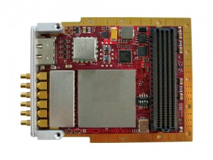

The FMC125 is a Quad-Channel Multi-Mode A/D FMC, fully compliant with VITA 57.1 Standards. The card provides four 8-bit ADC channels that enable simultaneous sampling of 4, 2, or 1 channel with a maximum sample rate of 1.25 GSPS (4-channel mode), 2.5 GSPS (2-channel mode), or 5.0 GSPS (1-channel mode).
The sample clock can be supplied externally through a coax connection or supplied by an internal clock source (optionally locked to an external reference). Additionally a trigger input for customized sampling control is available.
The FMC125 daughter card is mechanically and electrically compliant to the FMC standard as established by ANSI/VITA 57.1. The FMC125 has a HPC (high-pin count) 400-pin connector, front panel I/O, and can be used in a conduction cooled environment.
The design is based on the E2V Quad A/D EV8AQ160 chip-set having DDR LVDS outputs. The analog signal inputs are available on the front panel on coax connections and have individual calibration circuits for fine-tuning of gain, offset, and phase.
The FMC125 allows flexible control on clock source, sampling frequency, and calibration through the I2C serial communication bus. Furthermore the card is equipped with power supply and temperature monitoring and offers several power-down modes to switch off unused functions.
Features:
- Quad – Dual – Single 8-Bit Channel Operation
- 4-Channel 1.25 Gsps A/D conversion Mode
- 2-channel 2.50 Gsps A/D conversion Mode (calibration package required, option –C48 to be added to P/N)
- 1-channel 5.00 Gsps A/D conversion Mode (calibration package required, option –C48 to be added to P/N)
- VITA 57.1-2010 compliant.
- Conduction Cooled
- 1.25Gsps or 625Msps DDR LVDS outputs
- Coax front panel inputs on SSMC connectors
- Single ended AC-coupled analog input.
- Flexible clock tree enables:
- internal clock
- external clock
- Mil-I-46058c Conformal Coating Compliant (optional)
- HPC – High Pin Count Connector (400-pins)