
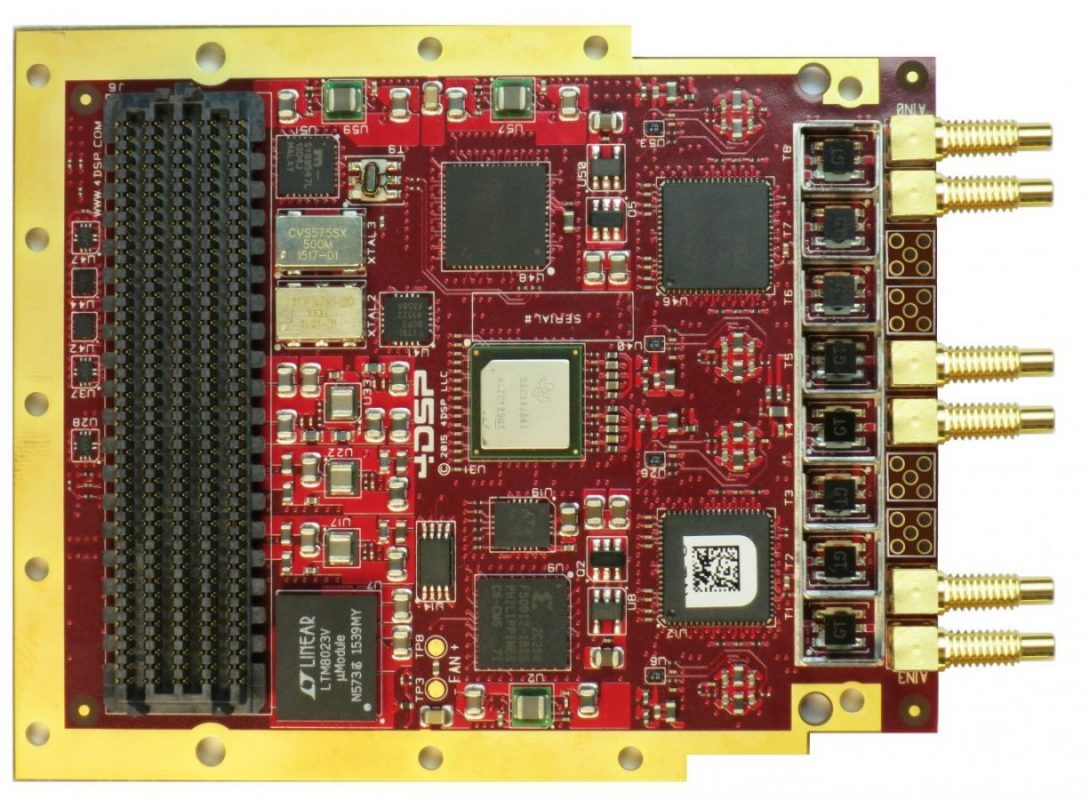
FMC-HPC ADC Board
Click for full size Image.
Two Channel 16-Bit A/D up to 1.0 Gsps
Two Channel 16-Bit D/A up to 1.4 Gsps
The FMC121 provides two 16-bit A/D channels up to 1Gsps and two 16-bit D/A channels up to 1.4 Gsps data rate with a 2.8 GSPS update rate. The design is based on Texas Instruments’ ADS54J60 Analog-to-Digital converter and Texas Instruments DAC39J84 Digital-to-Analog converter. The sample clock can be supplied externally through a coaxial connection or supplied by an internal clock source (optionally locked to an external reference) for multi-channel synchronization. An external trigger input is available for timing synchronization. The FMC121 is mechanically and electrically compliant to the FMC standard (ANSI/VITA 57.1). The card connects to an FPGA carrier card through a standard high-pin count (HPC) connector. Front panel I/O can optionally be populated with MMCX or SSMC coaxial connectors. Analog I/O is DC coupled. The FMC121 is designed to be used in convection or conduction cooled environments. When paired with the latest FPGA carrier cards such as the 4DSP PC821 with Xilinx Ultrascale technology, customers can develop innovative high performance algorithms on an industry standard platform
Features
- 2-Channels 16-bit 1.0 Gsps A/D
- 1.5Ghz Analog Bandwidth
- Usable in the 3rd Nyquist Zone
- 2-Channels 16-bit 1.4 Gsps D/A
- 2.8 GSPS Update Rate
- Onboard 48-bit NCO for flexible Signal Placement
- VITA 57.1 HPC compliant
- Conduction Cooled – Standard option
- DC coupled analog input and output
- Internal clock or external clock
- Mil-I-46058c Conformal Coating Complaint (optional)
- HPC – High Pin Count Connector
- 6 front panel SSMC or MMCX connectors
- 2Kbit EEPROM (M24CO2-WDW) accessible from the Host via I2C bus.